 | –≠–ª–µ–∫—Ç—Ä–æ–Ω–Ω—ã–π –∫–æ–º–ø–æ–Ω–µ–Ω—Ç: OP270 | –°–∫–∞—á–∞—Ç—å:  PDF PDF  ZIP ZIP |
ƒÓÍÛÏÂÌÚýˆËˇ Ë ÓÔËÒýÌˡ www.docs.chipfind.ru
REV. C
Information furnished by Analog Devices is believed to be accurate and
reliable. However, no responsibility is assumed by Analog Devices for its
use, nor for any infringements of patents or other rights of third parties that
may result from its use. No license is granted by implication or otherwise
under any patent or patent rights of Analog Devices. Trademarks and
registered trademarks are the property of their respective companies.
a
OP270
One Technology Way, P.O. Box 9106, Norwood, MA 02062-9106, U.S.A.
Tel: 781/329-4700
www.analog.com
Fax: 781/326-8703
© 2003 Analog Devices, Inc. All rights reserved.
Dual Very Low Noise Precision
Operational Amplifier
FEATURES
Very Low Noise 5 nV/
˜
˜
˜
˜
˜Hz @ 1 kHz Max
Excellent Input Offset Voltage 75 V Max
Low Offset Voltage Drift 1
V/ C Max
Very High Gain 1500 V/mV Min
Outstanding CMR 106 dB Min
Slew Rate 2.4 V/ s Typ
Gain Bandwidth Product 5 MHz Typ
Industry-Standard 8-Lead Dual Pinout
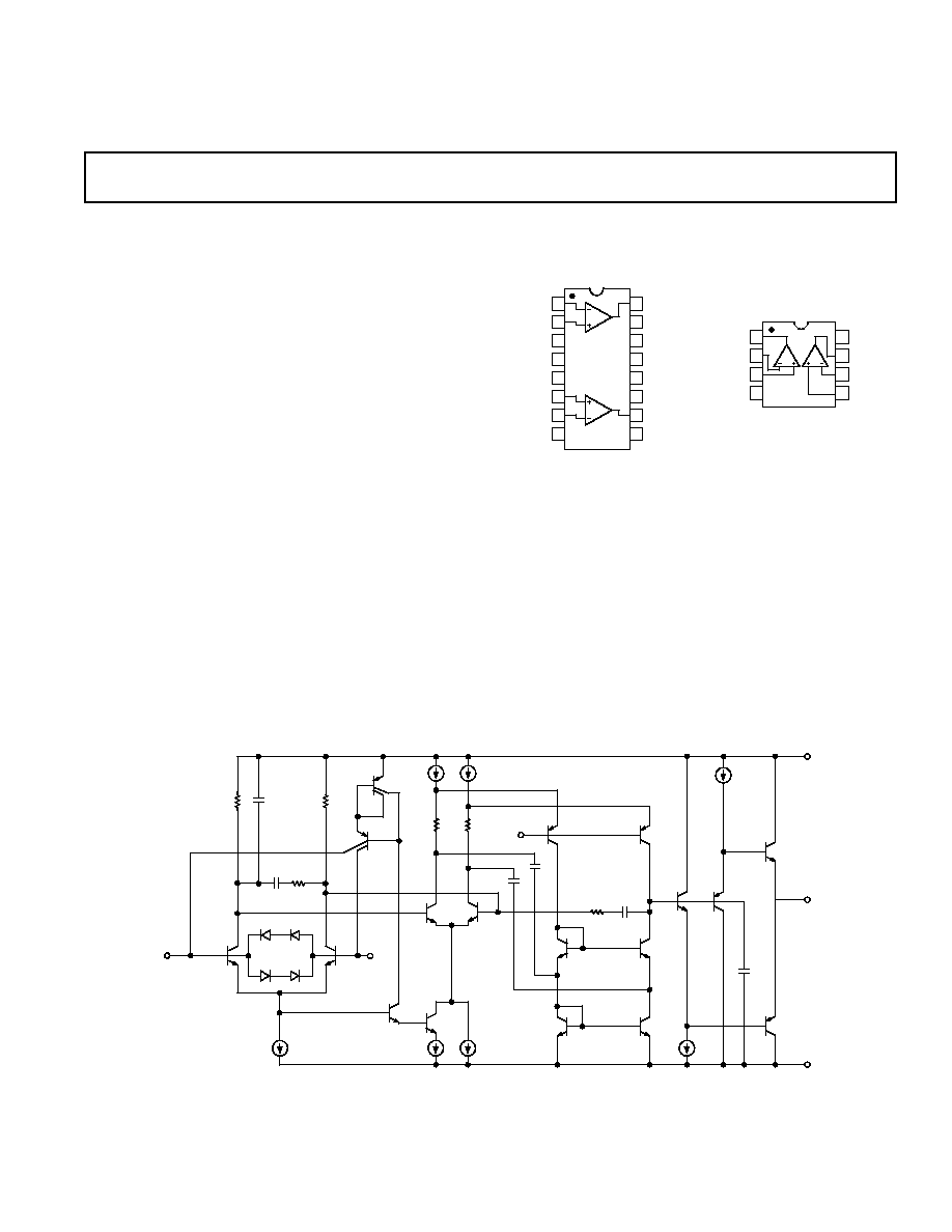
SIMPLIFIED SCHEMATIC
(One of Two Amplifiers Is Shown)
≠IN
+IN
BIAS
V+
OUT
V≠
GENERAL DESCRIPTION
The OP270 is a high performance, monolithic, dual operational
amplifier with exceptionally low voltage noise, 5 nV/
˜Hz max at
1 kHz. It offers comparable performance to ADI's industry
standard OP27.
The OP270 features an input offset voltage below 75
mV and an
offset drift under 1
mV/C, guaranteed over the full military tem-
perature range. Open-loop gain of the OP270 is over 1,500,000
into a 10 k
W load, ensuring excellent gain accuracy and linearity,
even in high gain applications. Input bias current is under 20 nA,
which reduces errors due to signal source resistance. The OP270's
CMR of over 106 dB and PSRR of less than 3.2
mV/V signifi-
cantly reduce errors due to ground noise and power supply
fluctuations. Power consumption of the dual OP270 is one-third
less than two OP27s, a significant advantage for power conscious
applications. The OP270 is unity-gain stable with a gain bandwidth
product of 5 MHz and a slew rate of 2.4 V/
ms.
The OP270 offers excellent amplifier matching, which is important
for applications such as multiple gain blocks, low noise instru-
mentation amplifiers, dual buffers, and low noise active filters.
The OP270 conforms to the industry-standard 8-lead DIP pinout.
It is pin compatible with the MC1458, SE5532/A, RM4558, and
HA5102 dual op amps, and can be used to upgrade systems
using those devices.
For higher speed applications, the OP271, with a slew rate of
8 V/
ms, is recommended. For a quad op amp, see the OP470.
CONNECTION DIAGRAMS
16-Lead SOIC
(S-Suffix)
1
2
3
4
5
6
7
8
NC = NO CONNECT
≠IN A
16
15
14
13
12
11
10
9
+IN A
NC
V≠
NC
+IN B
≠IN B
NC
OUT A
NC
NC
V+
NC
NC
OUT B
NC
OP270
8-Lead PDIP (P-Suffix)
8-Lead CERDIP
(Z-Suffix)
1
2
3
4
OUT A
8
7
6
5
≠IN A
+IN A
V≠
V+
OUT B
≠IN B
+IN B
A
B
OP270

REV. C
≠2≠
(V
S
=
15 V, T
A
= 25 C, unless otherwise noted.)
OP270≠SPECIFICATIONS
OP270E
OP270F
OP270G
PARAMETER
SYMBOL CONDITIONS
MIN TYP MAX
MIN
TYP
MAX
MIN
TYP MAX
UNIT
Input Offset Voltage
V
OS
10
75
20
150
50
250
mV
Input Offset Current
l
OS
V
CM
= 0 V
1
10
3
15
5
20
nA
Input Bias Current
I
B
V
CM
= 0 V
5
20
10
40
15
60
nA
Input Noise Voltage
e
n
p-p
0.1 Hz to 10 Hz
80
200
80
200
80
nV p-p
(Note 1)
Input Noise
f
O
= 10 Hz
3.6
6.5
3.6
6.5
3.6
nV/
˜
˜
˜
˜
˜Hz
Voltage Density
f
O
= 100 Hz
3.2
5.5
3.2
5.5
3.2
nV/
˜
˜
˜
˜
˜Hz
e
n
f
O
= 1 kHz
3.2
5.0
3.2
5.0
3.2
nV/
˜
˜
˜
˜
˜Hz
(Note 2)
Input Noise
f
O
= 10 Hz
1.1
1.1
1.1
pA/
˜
˜
˜
˜
˜Hz
Current Density
i
n
f
O
= 100 Hz
0.7
0.7
0.7
pA/
˜
˜
˜
˜
˜Hz
f
O
= 1 kHz
0.6
0.6
0.6
pA/
˜
˜
˜
˜
˜Hz
Large-Signal
V
O
=
±10 V
Voltage Gain
A
VO
R
L
= 10 k
W
1500 2300
1000 1700
750
1500
V/mV
R
L
= 2 k
W
750
1200
500
900
350
700
V/mV
Input Voltage Range
IVR
(Note3)
±12 ±12.5
±12 ±12.5
±12 ±12.5
V
Output Voltage Swing
V
O
R
L
2 kW
±12 ±13.5
±12 ±13.5
±12 ±13.5
V
Common-Mode
Rejection
CMR
V
CM
=
±11 V
106
125
100
120
90
110
dB
Power Supply
Rejection Ratio
PSRR
V
S
=
±4.5 V
0.56 3.2
1.0
5.6
1.5
6
mV/V
to
±18 V
Slew Rate
SR
1.7
2.4
1.7
2.4
1.7
2.4
V/
ms
Supply Current
I
SY
No Load
4
6.5
4
6.5
4
6.5
mA
(All Amplifiers)
Gain Bandwidth
GBP
5
5
5
MHz
Product
Channel Separation
CS
V
O
=
±20 V p-p
f
O
= 10 Hz
125
175
125
175
175
dB
(Note 1)
Input Capacitance
C
IN
3
3
3
pF
Input Resistance
R
IN
0.4
0.4
0.4
M
W
Differential-Mode
Input Resistance
R
INCM
20
20
20
G
W
Common-Mode
Settling Time
t
S
A
V
= +1, 10 V
5
5
5
ms
Step to 0.01%
NOTES
1. Guaranteed but not 100% tested.
2. Sample tested.
3. Guaranteed by CMR test.
Specifications subject to change without notice.
REV. C
≠3≠
ELECTRICAL SPECIFICATIONS
SPECIFICATIONS
OP270
(
Vs =
15 V, ≠40
C
£ T
A
£
85 C, unless otherwise noted.
)
OP270E
OP270F
OP270G
PARAMETER
SYMBOL
CONDITIONS
MIN TYP MAX
MIN
TYP
MAX
MIN
TYP MAX
UNIT
Input Offset Voltage
V
OS
25
150
45
275
100
400
mV
Average Input
Offset Voltage Drift
TCV
OS
0.2
1
0.4
2
0.7
3
mV/C
Input Offset Current
I
OS
V
CM
= 0 V
1.5
30
5
40
15
50
nA
Input Bias Voltage
I
B
V
CM
= 0 V
6
60
15
70
19
80
nA
Large-Signal
V
O
=
±10 V
Voltage Gain
A
VO
R
L
= 10 k
W
1000 1800
600
1400
400
1250
V/mV
R
L
= 2 k
W
500
900
300
700
225
670
V/mV
Input Voltage Range
*
IVR
±12 ±12.5
±12 ±12.5
±12 ±12.5
V
Output Voltage Swing
V
O
R
L
2 kW
±12 ±13.5
±12 ±13.5
±12 ±13.5
V
Common-Mode
Rejection
CMR
V
CM
=
±11 V
100
120
94
115
90
100
dB
Power Supply
Rejection Ratio
PSRR
V
S
=
±4.5 V
0.7
5.6
1.8
10
2.0
1.5
mV/V
to
±18 V
Supply Current
I
SY
No Load
4.4
7.2
4.4
7.2
4.4
7.2
mA
(All Amplifiers)
* Guaranteed by CMR test.
Specifications subject to change without notice.
REV. C
OP270
≠4≠
ABSOLUTE MAXIMUM RATINGS
1
Supply Voltage . . . . . . . . . . . . . . . . . . . . . . . . . . . . . . . .
±18 V
Differential Input Voltage
2
. . . . . . . . . . . . . . . . . . . . . .
±1.0 V
Differential Input Current
2
. . . . . . . . . . . . . . . . . . . .
±25 mA
Input Voltage . . . . . . . . . . . . . . . . . . . . . . . . . . Supply Voltage
Output Short-Circuit Duration . . . . . . . . . . . . . . . Continuous
Storage Temperature Range
P, S, Z Package . . . . . . . . . . . . . . . . . . . . ≠65
∞C to +150∞C
Lead Temperature Range (Soldering, 60 sec) . . . . . . . . 300
∞C
Junction Temperature (T
J
) . . . . . . . . . . . . . ≠65
∞C to +150∞C
ORDERING GUIDE
T
A
= +25
∞
C
V
OS
Max
JC
JA
*
Temperature
Package
Package
Model
( V)
(
∞
C/W)
(
∞
C/W)
Range
Description
Option
OP270EZ
75
12
134
XIND
8-Lead CERDIP
Q-8 (Z-Suffix)
OP270FZ
150
12
134
XIND
8-Lead CERDIP
Q-8 (Z-Suffix)
OP270GP
250
37
96
XIND
8-Lead PDIP
N-8 (P-Suffix)
OP270GS
250
27
92
XIND
16-Lead SOIC
RW-16 (S-Suffix)
*
JA
is specified for worst-case mounting conditions, i.e.,
JA
is specified for device
in socket for CERDIP and PDIP packages;
JA
is specified for device soldered to
printed circuit board for SOIC package.
Operating Temperature Range
OP270E, OP270F, OP270G . . . . . . . . . . . ≠40
∞C to +85∞C
NOTES
1
Stresses above those listed under Absolute Maximum Ratings may cause perma-
nent damage to the device. This is a stress rating only; functional operation of the
device at these or any other conditions above those listed in the operational
sections of this specification is not implied. Exposure to absolute maximum rating
conditions for extended periods may affect device reliability.
2
The OP270's inputs are protected by back-to-back diodes. Current limiting
resistors are not used, in order to achieve low noise performance. If differential
voltage exceeds +10 V, the input current should be limited to
±25 mA.
For military processed devices, please refer to the Standard
Microcircuit Drawing (SMD) available at
www.dscc.dla.mil/programs/milspec/default.asp.
SMD Part Number
ADI Equivalent
5962-8872101PA
OP270AZMDA
WARNING!
ESD SENSITIVE DEVICE
CAUTION
ESD (electrostatic discharge) sensitive device. Electrostatic charges as high as 4000 V readily
accumulate on the human body and test equipment and can discharge without detection. Although
the OP270 features proprietary ESD protection circuitry, permanent damage may occur on devices
subjected to high energy electrostatic discharges. Therefore, proper ESD precautions are
recommended to avoid performance degradation or loss of functionality.
REV. C
≠5≠
OP270
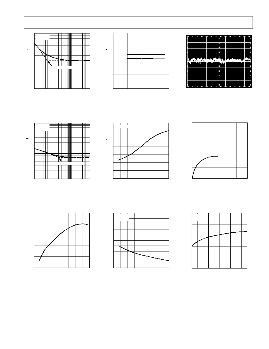
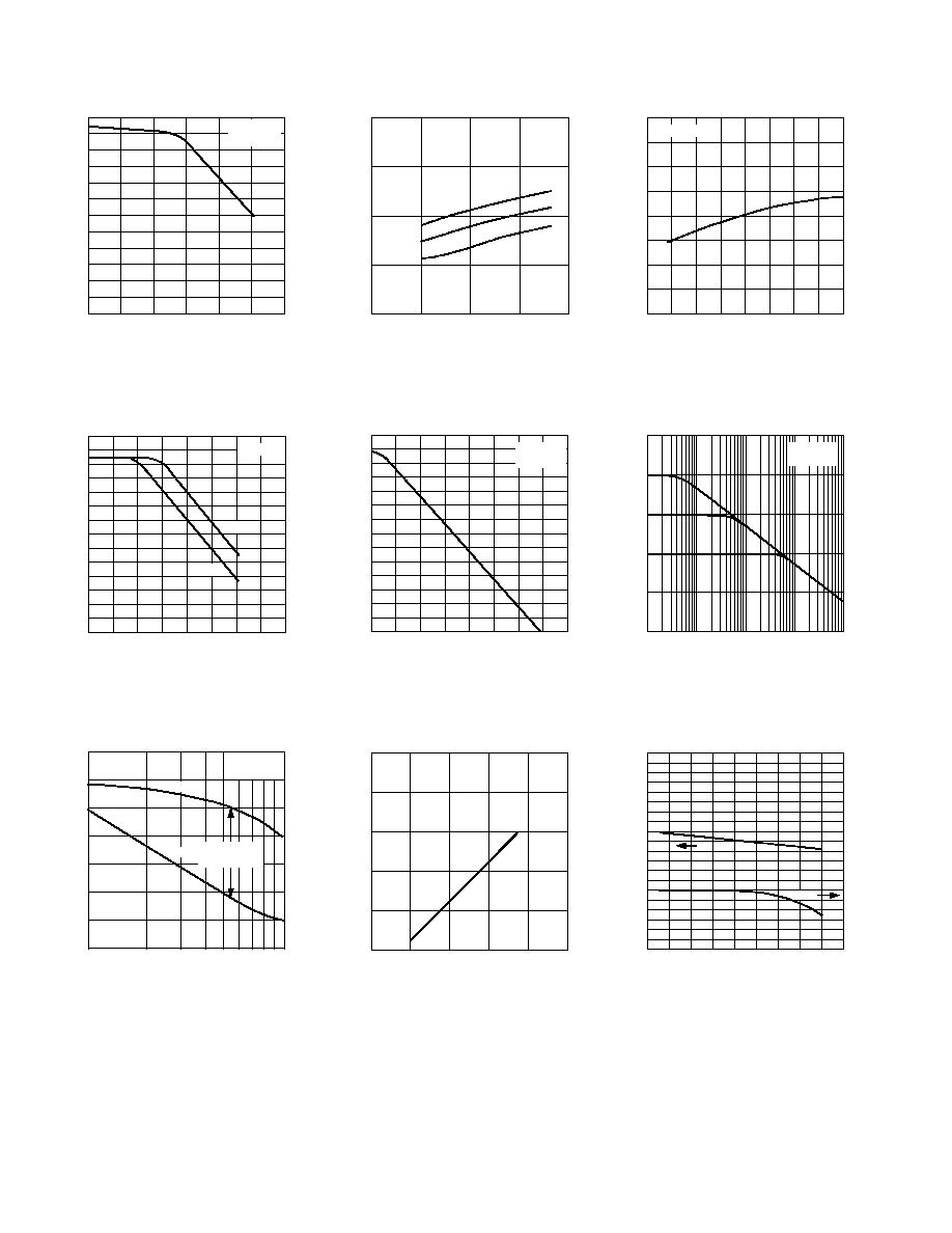
FREQUENCY (Hz)
VO
LTA
G
E
NOISE (nV/
Hz)
10
1
10
100
1k
1
1/f CORNER = 5Hz
T
A
= 25 C
V
S
= 15V
2
3
4
5
7
9
8
6
TPC 1. Voltage Noise Density
vs. Frequency
FREQUENCY (Hz)
CURRENT NOISE (pA/
Hz)
10
10
100
10k
0.1
1.0
1k
T
A
= 25 C
V
S
= 15V
1/f CORNER = 200Hz
TPC 4. Current Noise Density
vs. Frequency
TEMPERATURE ( C)
INPUT BIAS CURRENT (nA)
7
≠75
2
4
≠50
0
50
100
125
3
6
V
S
= 15V
V
CM
= 0V
5
≠25
25
75
TPC 7. Input Bias Current vs.
Temperature
SUPPLY VOLTAGE (V)
VO
LTA
G
E
NOISE (nV/
Hz)
5
0
5
15
20
1
2
3
4
10
T
A
= 25 C
AT 10Hz
AT 1kHz
TPC 2. Voltage Noise Density
vs. Supply Voltage
TEMPERATURE ( C)
VO
LTA
G
E
NOISE (nV/
Hz)
40
≠75
≠30
≠10
10
30
≠50
≠25
0
25
50
75
100
125
≠20
0
20
V
S
= 15V
TPC 5. Input Offset Voltage vs.
Temperature
TEMPERATURE ( C)
INPUT OFFSET CURRENT (nA)
5
≠75
0
2
≠50
0
50
100
125
1
4
V
S
= 15V
V
CM
= 0V
3
≠25
25
75
TPC 8. Input Offset Current vs.
Temperature
T
A
= 25 C
V
S
= 15V
NOISE V
OL
T
A
GE
(100nV/DIV)
0.1Hz TO 10Hz NOISE
TIME (1sec/DIV)
TPC 3. 0.1 Hz to 10 Hz Input
Voltage Noise
TIME (Minutes)
CHANGE IN OFFSET
V
OL
T
A
GE (
A)
5
0
0
2
1
2
3
4
5
1
4
T
A
= 25 C
V
S
= 15V
3
TPC 6. Warm-Up Offset Voltage
Drift
COMMON-MODE VOLTAGE (V)
INPUT BIAS CURRENT (nA)
7
≠12.5
2
4
3
6
T
A
= 25 C
V
S
= 15V
5
≠10.0
≠7.5
≠5.0
≠2.5
0.0
2.5
5.0
7.5
10.0
12.5
TPC 9. Input Bias Current vs.
Common-Mode Voltage
Typical Performance Characteristics≠
REV. C
OP270
≠6≠
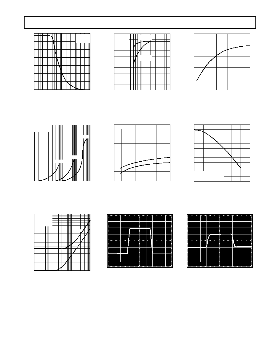
FREQUENCY (Hz)
CMR (dB)
130
10
60
40
110
T
A
= 25 C
V
S
= 15V
80
1
10
100
1k
10k
100k
1M
120
100
90
70
50
30
20
TPC 10. CMR vs. Frequency
FREQUENCY (Hz)
PSR (dB)
140
0
1
100
10k
1M
100M
T
A
= 25 C
10
1k
100k
10M
20
40
60
80
100
120
≠PSR
+PSR
TPC 13. PSR vs. Frequency
FREQUENCY (Hz)
GAIN (dB)
25
≠10
1
≠5
0
5
15
10
20
T
A
= 25 C
V
S
= 15V
PHASE
GAIN
PHASE
MARGIN = 62
80
180
160
120
140
100
PHASE SHIFT (Degrees)
2
3
4
5
6 7 8 9 10
TPC 16. Open-Loop Gain Phase
Shift vs. Frequency
SUPPLY VOLTAGE (V)
TO
TA
L SUPPL
Y CURRENT (mA)
6
2
3
0
5
10
15
20
5
4
+125 C
+25 C
≠55 C
TPC 11. Total Supply Current
vs. Supply Voltage
FREQUENCY (Hz)
VO
LTA
GE GAIN (dB)
140
0
1
100
10k
1M
100M
T
A
= 25 C
V
S
= 15V
10
1k
100k
10M
20
40
60
80
100
120
TPC 14. Open-Loop Gain vs.
Frequency
SUPPLY VOLTAGE (V)
OPEN-LOOP GAIN (V/mV)
5000
0
0
1000
2000
3000
4000
5
10
15
20
25
TPC 17. Open-Loop Gain vs.
Supply Voltage
TEMPERATURE ( C)
TO
TA
L SUPPL
Y CURRENT (mA)
8
0
2
≠75
≠25
25
75
125
6
4
V
S
= 15V
≠50
0
50
100
7
1
5
3
TPC 12. Total Supply Current
vs. Temperature
FREQUENCY (Hz)
CLOSED-LOOP GAIN (dB)
80
≠20
1k
10k
T
A
= 25 C
V
S
= 15V
100k
10M
0
20
40
60
1M
TPC 15. Closed-Loop Gain vs.
Frequency
TEMPERATURE ( C)
PHASE MARGIN (Degrees)
80
40
≠75
50
60
70
≠50 ≠25
0
25
50
75
100 125 150
8
7
6
5
4
GAIN B
AND
WIDTH PR
ODUCT (MHz)
GBP
TPC 18. Gain-Bandwidth Phase
Margin vs. Temperature
REV. C
≠7≠
OP270
FREQUENCY (Hz)
PEAK-T
O-PEAK AMPLITUDE (V)
28
0
1k
8
12
20
10k
100k
1M
10M
4
16
24
T
A
= 25 C
V
S
= 15V
THD = 1%
TPC 19. Maximum Output
Swing vs. Frequency
FREQUENCY (Hz)
OUTPUT IMPED
ANCE (
)
0
1k
100k
10M
25
50
75
100
10k
1M
T
A
= +25 C
V
S
= 15V
A
V
= 100
A
V
= 10
A
V
= 1
TPC 22. Output Impedance vs.
Frequency
FREQUENCY (Hz)
DIST
OR
TION (%)
0.001
10
10k
0.1
1k
T
A
= 25 C
V
S
= 15V
V
O
= 20V p-p
R
L
=2k
100
0.01
A
V
= 10
A
V
= 1
TPC 25. Total Harmonic Distor-
tion vs. Frequency
LOAD RESISTANCE ( )
MAXIMUM OUTPUT (
V)
5
1k
10k
100k
T
A
= 25 C
V
S
= 15V
6
7
8
9
10
11
12
13
14
15
NEGATIVE
SWING
POSITIVE
SWING
TPC 20. Maximum Output
Voltage vs. Load Resistance
TEMPERATURE ( C)
SLEW RA
TE (V/
s)
2.2
≠75
25
125
2.5
2.8
≠25
75
V
S
= 15V
≠SR
+SR
0
100
≠50
50
2.3
2.4
2.6
2.7
TPC 23. Slew Rate vs.
Temperature
T
A
= 25 C
V
S
= 15V
A
V
= +1
R
L
= 2k
5V
20 s
TPC 26. Large Signal Transcient
Response
CAPACITIVE LOAD (pF)
O
VERSHOO
T (%)
0
0
400
1000
T
A
= 25 C
V
S
= 15V
V
IN
= 100mV
A
V
= +1
10
20
30
40
50
200
600
800
TPC 21. Small-Signal Overshoot
vs. Capacitive Load
FREQUENCY (Hz)
CHANNEL SEP
ARA
TION (dB)
70
1
1k
1M
130
190
10k
T
A
= 25 C
V
S
= 15V
V
O
= 20V p-p TO 10kHz
100
100k
10
90
110
150
170
120
180
80
100
140
160
TPC 24. Channel Separation vs.
Frequency
T
A
= 25 C
V
S
= 15V
A
V
= +1
R
L
= 2k
50mV
200nS
TPC 27. Small-Signal
Transient Response
REV. C
OP270
≠8≠
1/2
OP270
V
1
20V
p-p
5k
500
5k
50
V
2
1/2
OP270
CHANNEL SEPARATION = 20 log
V
1
V
2
/1000
Figure 1. Channel Separation Test Circuit
1/2
OP270
1/2
OP270
7
1
8
5
6
3
2
100k
100k
200k
4
+18V
≠18V
Figure 2. Burn-In Circuit
APPLICATIONS INFORMATION
VOLTAGE AND CURRENT NOISE
The OP270 is a very low noise dual op amp, exhibiting atypical
voltage noise of only 3.2 nV/
˜
˜
˜
˜
˜Hz @ 1 kHz. The exceptionally
low noise characteristic of the OP270 is achieved in part by
operating the input transistors at high collector currents since
the voltage noise is inversely proportional to the square root of
the collector current. Current noise, however, is directly propor-
tional to the square root of the collector current. As a result, the
outstanding voltage noise performance of the OP270 is gained
at the expense of current noise performance, which is normal for
low noise amplifiers.
To obtain the best noise performance in a circuit, it is vital to
understand the relationship between voltage noise (e
n
), current
noise (i
n
), and resistor noise (e
t
).
TOTAL NOISE AND SOURCE RESISTANCE
The total noise of an op amp can be calculated by:
E
e
i R
e
n
n
n
S
t
=
( )
+
( )
+
( )
2
2
2
where:
E
n
= total input referred noise
e
n
= op amp voltage noise
i
n
= op amp current noise
e
t
= source resistance thermal noise
R
S
= source resistance
The total noise is referred to the input and at the output would
be amplified by the circuit gain.
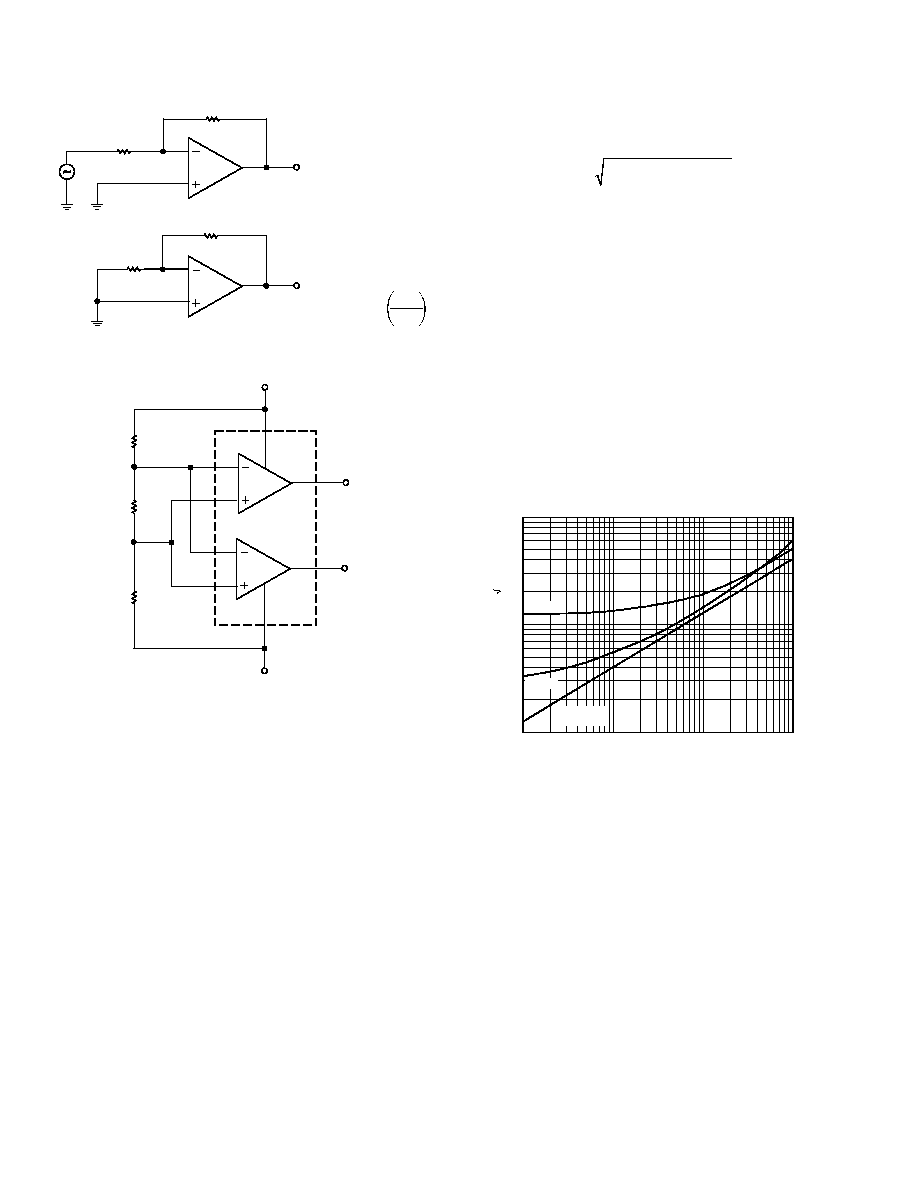
Figure 3 shows the relationship between total noise at 1 kHz
and source resistance. For R
S
< 1 k
W the total noise is dominated
by the voltage noise of the OP270. As R
S
rises above 1 k
W, total
noise increases and is dominated by resistor noise rather than by
the voltage or current noise of the OP270. When R
S
exceeds
20 k
W, current noise of the OP270 becomes the major contributor
to total noise.
R
S
≠ SOURCE RESISTANCE ( )
100
100
1k
10k
100k
TOT
A
L
NOISE (nV/
Hz)
1
10
OP270
RESISTOR
NOISE ONLY
OP200
Figure 3. Total Noise vs. Source Resistance
(Including Resistor Noise) at 1 kHz
Figure 4 also shows the relationship between total noise and
source resistance, but at 10 Hz. Total noise increases more
quickly than shown in Figure 3 because current noise is inversely
proportional to the square root of frequency. In Figure 4, current
noise of the OP270 dominates the total noise when R
S
> 5 k
W.
Figures 3 and 4 show that to reduce total noise, source resistance
must be kept to a minimum. In applications with a high source
resistance, the OP200, with lower current noise than the OP270,
will provide lower total noise.
REV. C
OP270
≠9≠
R
S
≠ SOURCE RESISTANCE ( )
100
100
1k
10k
100k
TOT
A
L
NOISE (nV/
Hz)
1
10
RESISTOR
NOISE ONLY
OP200
OP270
Figure 4. Total Noise vs. Source Resistance
(Including Resistor Noise) at 10 Hz
R
S
≠ SOURCE RESISTANCE ( )
1000
100
1k
10k
100k
PEAK-T
O-PEAK NOISE (nV)
10
100
RESISTOR
NOISE ONLY
OP200
OP270
Figure 5. Peak-to-Peak Noise (0.1 Hz to 10 Hz) vs.
Source Resistance (Includes Resistor Noise)
Figure 5 shows peak-to-peak noise versus source resistance over the
0.1 Hz to 10 Hz range. Once again, at low values of R
S
, the voltage
noise of the OP270 is the major contributor to peak-to-peak
noise, with current noise the major contributor as R
S
increases.
The crossover point between the OP270 and the OP200 for
peak-to-peak noise is at R
S
= 17 k
W.
The OP271 is a higher speed version of the OP270, with a slew
rate of 8 V/
ms. Noise of the OP271 is slightly higher than that of
the OP270. Like the OP270, the OP271 is unity-gain stable.
For reference, typical source resistances of some signal sources
are listed in Table I.
Table I.
Source
Device
Impedance
Comments
Strain gage
<500
W
Typically used in low
frequency applications.
Magnetic
<1500
W
Low I
B
very important to reduce
tapehead,
self-magnetization problems
microphone
when direct coupling is used.
OP270 I
B
can be neglected.
Magnetic
<1500
W
Similar need for low I
B
in
phonograph
direct coupled applications.
cartridge
OP270 will not introduce any
self-magnetization problem.
Linear variable <1500
W
Used in rugged servo-feedback
differential
applications. Bandwidth of
transformer
interest is 400 Hz to 5 kHz.
R1
5
R2
5
OP270
DUT
≠
+
R3
1.24k
OP27E
≠
+
R4
200
R5
909
C1
2 F
R6
600
R8
10k
D1, D2
1N4148
OP27E
≠
+
R9
306k
C2
0.032 F
R10
65.4k
R11
65.4k
C4
0.22 F
C3
0.22 F
OP42E
≠
+
R12
10k
R13
5.9k
R14
4.99k
C5
1 F
e
OUT
GAIN = 50,000
V
S
= 15V
Figure 6. Peak-to-Peak Voltage Noise Test Circuit (0.1 Hz to 10 Hz)
REV. C
OP270
≠10≠
NOISE MEASUREMENTS
Peak-to-Peak Voltage Noise
The circuit of Figure 6 is a test setup for measuring peak-to-peak
voltage noise. To measure the 200 nV peak-to-peak noise specifica-
tion of the OP270 in the 0.1 Hz to 10 Hz range, the following
precautions must be observed:
1. The device has to be warmed up for at least five minutes. As
shown in the warm-up drift curve, the offset voltage typically
changes 2
mV due to increasing chip temperature after power-up.
In the 10-second measurement interval, these temperature
induced effects can exceed tens of nanovolts.
2. For similar reasons, the device has to be well shielded from
air currents. Shielding also minimizes thermocouple effects.
3. Sudden motion in the vicinity of the device can also "feed
through" to increase the observed noise.
4. The test time to measure noise of 0.1 Hz to 10 Hz should not
exceed 10 seconds. As shown in the noise-tester frequency
response curve of Figure 7, the 0.1 Hz corner is defined by
only one pole. The test time of 10 seconds acts as an additional
pole to eliminate noise contribution from the frequency band
below 0.1 Hz.
FREQUENCY (Hz)
100
0.01
0.1
1.0
10
100
GAIN (dB)
80
60
40
20
0
Figure 7. 0.1 Hz to 10 Hz Peak-to-Peak Voltage
Noise Test Circuit Frequency Response
5. A noise-voltage-density test is recommended when measuring
noise on a large number of units. A 10 Hz noise-voltage-density
measurement will correlate well with a 0.1 Hz to 10 Hz
peak-to-peak noise reading, since both results are determined by
the white noise and the location of the 1/f corner frequency.
6. Power should be supplied to the test circuit by well bypassed
low noise supplies, e.g., batteries. They will minimize output
noise introduced via the amplifier supply pins.
Noise Measurement -- Noise Voltage Density
The circuit of Figure 8 shows a quick and reliable method of
measuring the noise voltage density of dual op amps. The first
amplifier is in unity-gain, with the final amplifier in a noninverting
gain of 101. As noise voltages of each amplifier are uncorrelated,
they add in rms fashion to yield:
e
e
e
OUT
nA
2
nB
2
=
( )
+
( )
À
¡
^
Ø
~
101
The OP270 is a monolithic device with two identical amplifi-
ers. The noise voltage density of each individual amplifier will
match, giving:
e
e
e
OUT
n
2
n
=
À
¡
^
Ø
~ =
( )
101
2
101
2
1/2
OP270
≠
+
R1
100
1/2
OP270
≠
+
R2
10k
e
OUT
e
OUT
(nV/
Hz)
=
101 (
2
e
n
)
V
S
= 15V
TO SPECTRUM ANALYZER
Figure 8. Noise Voltage Density Test Circuit
OP270
DUT
≠
+
R3
1.24k
R2
100k
R1
5
OP27E
≠
+
R5
8.06k
e
nOUT
TO SPECTRUM ANALYZER
R4
200
GAIN = 10,000
V
S
= 15V
Figure 9. Current Noise Density Test Circuit
Noise Measurement -- Current Noise Density
The test circuit shown in Figure 9 can be used to measure cur-
rent noise density. The formula relating the voltage output to
current noise density is:
i
e
G
nV
Hz
R
n
nOUT
S
=
À
¡
^
Ø
~ -
(
)
2
2
40
/
where:
G = gain of 10,000
R
S
= 100 k
W source resistance
REV. C
OP270
≠11≠
CAPACITIVE LOAD DRIVING AND POWER SUPPLY
CONSIDERATIONS
The OP270 is unity-gain stable and capable of driving large
capacitive loads without oscillating. Nonetheless, good supply
bypassing is highly recommended. Proper supply bypassing
reduces problems caused by supply line noise and improves the
capacitive load driving capability of the OP270.
In the standard feedback amplifier, the op amp's output resis-
tance combines with the load capacitance to form a low-pass
filter that adds phase shift in the feedback network and reduces
stability. A simple circuit to eliminate this effect is shown in
Figure 10. The added components, C1 and R3, decouple the
amplifier from the load capacitance and provide additional
stability. The values of C1 and R3 shown in Figure 10 are for a
load capacitance of up to 1,000 pF when used with the OP270.
OP270
≠
+
R1
V
IN
R3
50
C1
200pF
R2
V
OUT
C1
1000pF
PLACE SUPPLY DECOUPLING
CAPACITOR AT OP270
C5
0.1 F
C4
10 F
+
V≠
C3
0.1 F
C2
10 F
+
V+
Figure 10. Driving Large Capacitive Loads
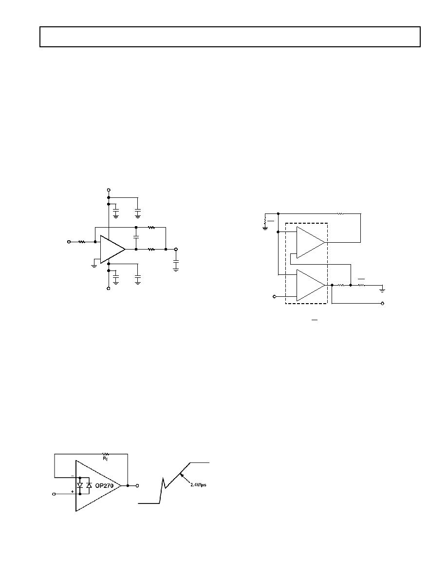
UNITY-GAIN BUFFER APPLICATIONS
When R
f
£ 100 W and the input is driven with a fast, large
signal pulse (>1 V), the output waveform will look like the one
in Figure 11.
During the fast feedthrough-like portion of the output, the input
protection diodes effectively short the output to the input, and a
current, limited only by the output short-circuit protection, will be
drawn by the signal generator. With R
f
500 W, the output is
capable of handling the current requirements (I
L
£ 20 mA at 10 V);
the amplifier will stay in its active mode and a smooth transition
will occur.
When R
f
> 3 k
W, a pole created by R
f
and the amplifier's input
capacitance (3 pF) creates additional phase shift and reduces
phase margin. A small capacitor (20 pF to 50 pF) in parallel
with R
f
helps eliminate this problem.
Figure 11. Pulsed Operation
APPLICATIONS
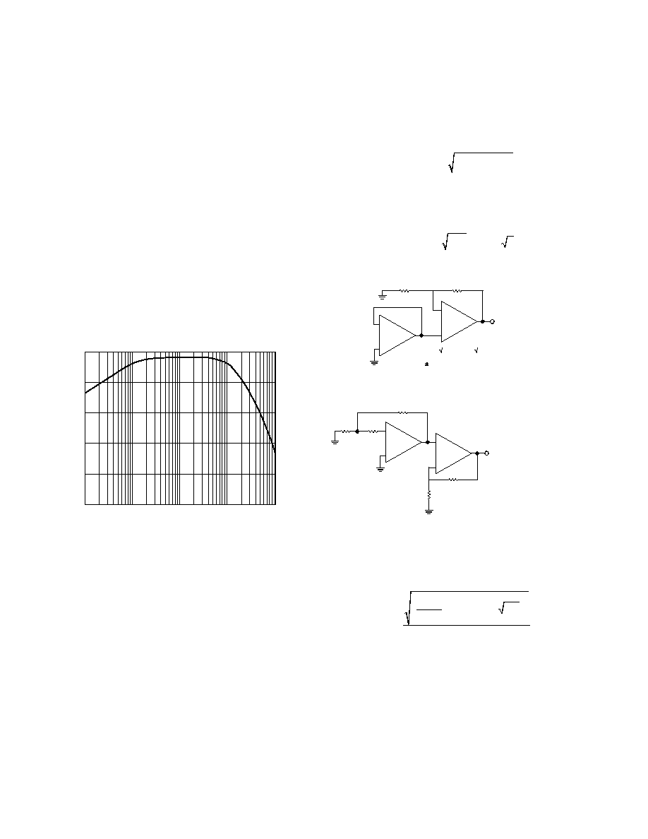
Low Phase Error Amplifier
The simple amplifier depicted in Figure 12 utilizes a monolithic
dual operational amplifier and a few resistors to substantially
reduce phase error compared to conventional amplifier designs.
At a given gain, the frequency range for a specified phase accuracy is
over a decade greater than for a standard single op amp amplifier.
The low phase error amplifier performs second-order frequency
compensation through the response of op amp A2 in the feed-
back loop of A1. Both op amps must be extremely well matched
in frequency response. At low frequencies, the A1 feedback
loop forces V
2
/(K1 + 1) = V
IN
. The A2 feedback loop forces
Vo/(K1 + 1) = V
2
/(K1 + 1), yielding an overall transfer function
of V
O
/V
IN
= K1 + 1. The dc gain is determined by the resistor
divider at the output, V
O
, and is not directly affected by the resis-
tor divider around A2. Note that like a conventional single op amp
amplifier, the dc gain is set by resistor ratios only. Minimum
gain for the low phase error amplifier is 10.
1/2
OP270E
A2
≠
+
1/2
OP270E
A1
≠
+
R2
K1
R2
R2 = R1
V
2
R2
R1
K1
V
O
V
O
= (K
1
+ 1) V
IN
ASSUME A1 AND A1 ARE MATCHED.
A
O
(s) =
T
s
V
IN
Figure 12. Low Phase Error Amplifier
Figure 13 compares the phase error performance of the low
phase error amplifier with a conventional single op amp ampli-
fier and a cascaded two-stage amplifier. The low phase error
amplifier shows a much lower phase error, particularly for fre-
quencies where
w/bw
T
< 0.1. For example, phase error of ≠0.1
occurs at 0.002
w/bw
T
for the single op amp amplifier, but at
0.11
w/bw
T
for the low phase error amplifier.
REV. C
OP270
≠12≠
FREQUENCY RATIO (1/
)( /
T
)
0
0.001
0.01
0.1
1.0
PHASE SHIFT (Degrees)
≠2
≠4
≠5
≠6
≠7
≠1
≠3
0.005
0.05
0.5
LOW PHASE ERROR
AMPLIFIER
CASCADED
(TWO STAGES)
SINGLE OP AMP.
CONVENTIONAL DESIGN
Figure 13. Phase Error Comparison
R3
680
C2
6.8 F
+
TANTALUM
R4
1k
60Hz
L1
1H
R5
680
C3
1 F
+
TANTALUM
R6
1k
200Hz
L2
600mH
R7
680
C4
0.22 F
R8
1k
800Hz
L3
180mH
R9
680
C5
0.047 F
R10
1k
3kHz
L4
60mH
R11
680
C6
0.022 F
R12
1k
10kHz
L5
10mH
1/2
OP270E
≠
+
C1
0.47 F
R1
47k
V
IN
R2
3.3k
1/2
OP270E
≠
+
R14
100
R13
3.3k
V
OUT
Figure 14. 5-Band Low Noise Graphic Equalizer
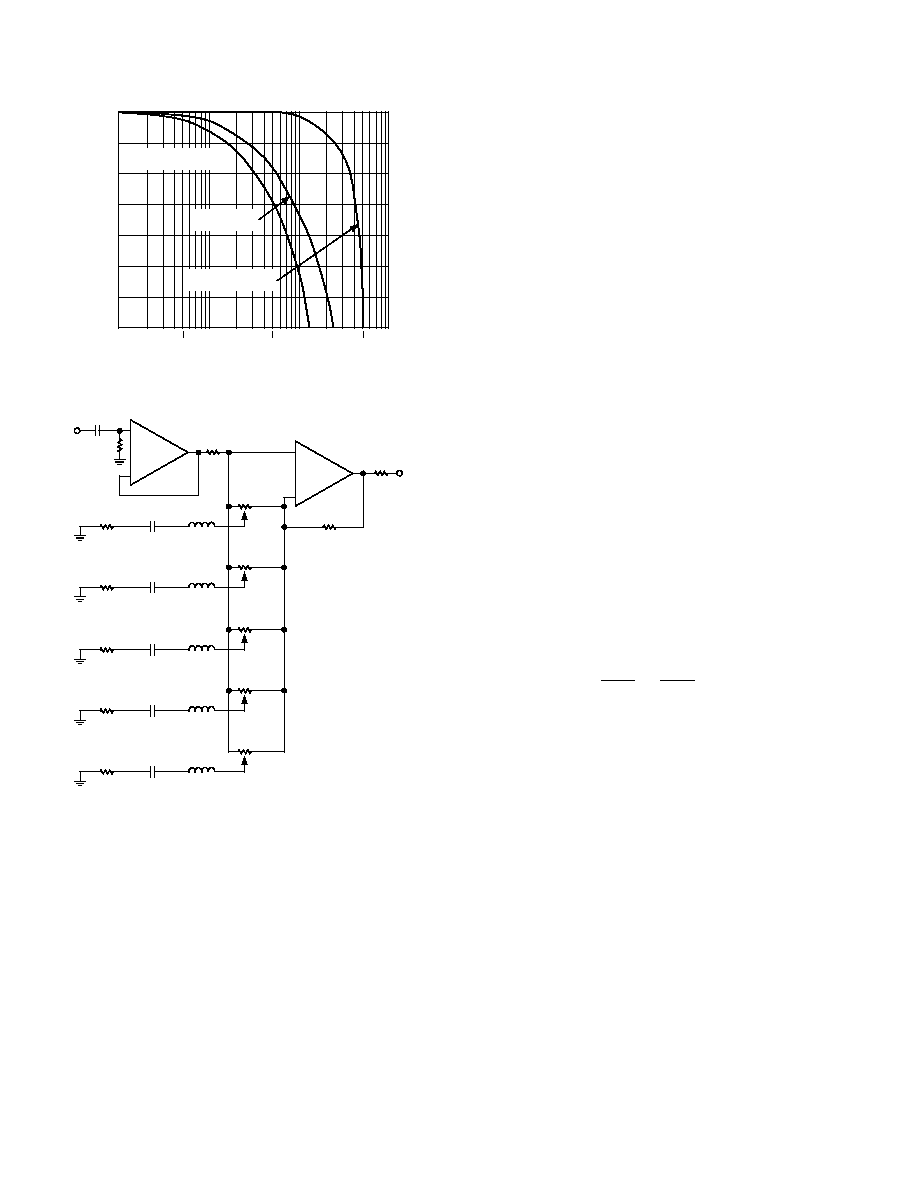
FIVE-BAND LOW NOISE STEREO GRAPHIC EQUALIZER
The graphic equalizer circuit shown in Figure 14 provides 15 dB of
boost or cut over a 5-band range. Signal-to-noise ratio over a 20 kHz
bandwidth is better than 100 dB and referred to a 3 V rms input.
Larger inductors can be replaced by active inductors, but this
reduces the signal-to-noise ratio.
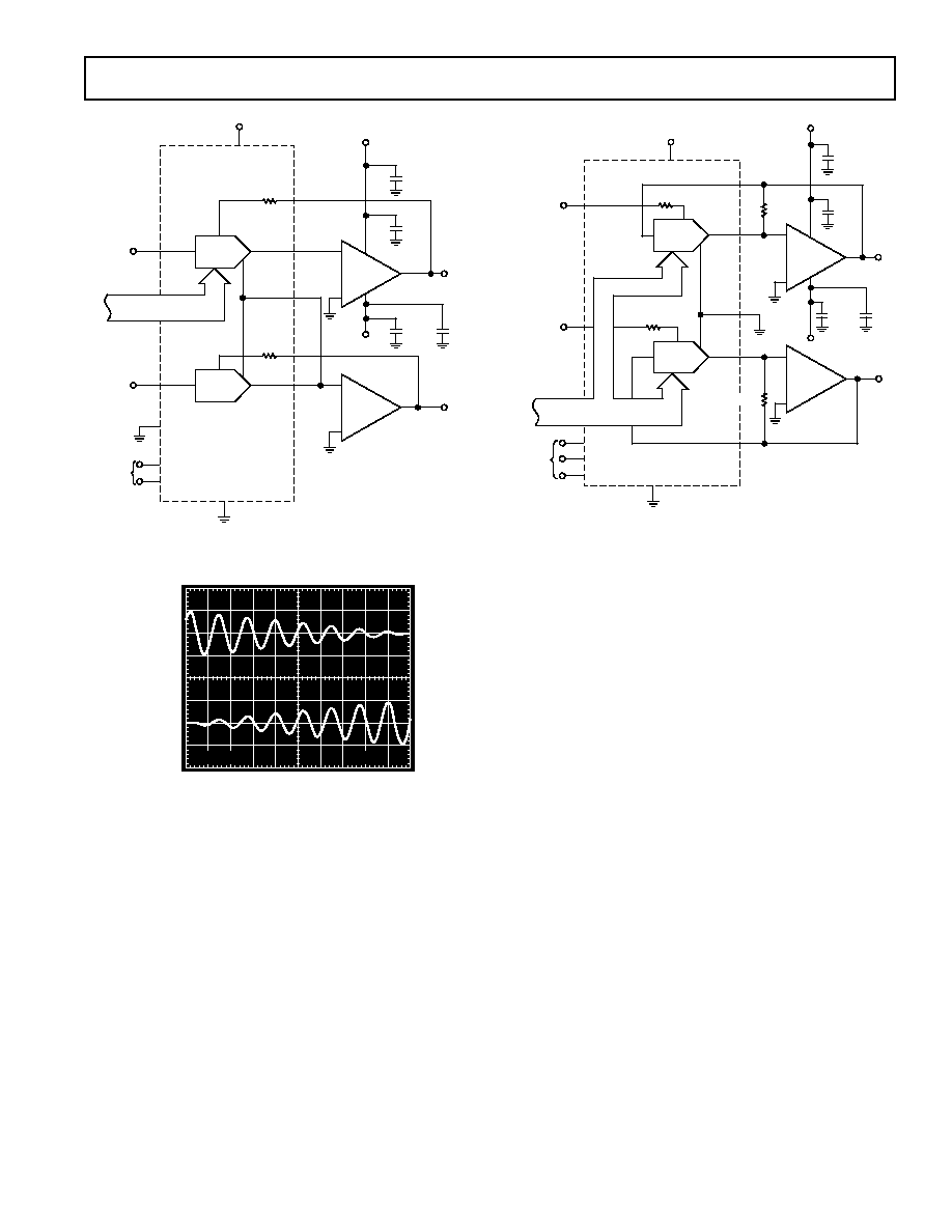
DIGITAL PANNING CONTROL
Figure 15 uses a DAC8221, a dual 12-bit CMOS DAC, to pan
a signal between two channels. One channel is formed by the
current output of DAC A driving one-half of an OP270 in a
current-to-voltage converter configuration. The other channel is
formed by the complementary output current of DAC A, which
normally flows to ground through the AGND pin. This comple-
mentary current is converted to a voltage by the other half of the
OP-270, which also holds AGND at virtual ground.
Gain error due to mismatching between the internal DAC ladder
resistors and the current-to-voltage feedback resistors is elimi-
nated by using feedback resistors internal to the DAC8221. Only
DAC A passes a signal; DAC B provides the second feedback
resistor. With V
REF
B unconnected, the current-to-voltage converter,
using R
FB
B, is accurate and not influenced by digital data reach-
ing DAC B. Distortion of the digital panning control is less than
0.002% over the 20 Hz to 20 kHz audio range. Figure 16 shows
the complementary outputs for a 1 kHz input signal and a digital
ramp applied to the DAC data input.
DUAL PROGRAMMABLE GAIN AMPLIFIER
The dual OP270 and the DAC8221, a dual 12-bit CMOS
DAC, can be combined to form a space-saving dual program-
mable amplifier. The digital code present at the DAC, which is
easily set by a microprocessor, determines the ratio between the
internal feedback resistor and the resistance the DAC ladder
presents to the op amp feedback loop. Gain of each amplifier is
V
V
n
OUT
IN
= ≠
4096
where n equals the decimal equivalent of the 12-bit digital code
present at the DAC. If the digital code present at the DAC
consists of all zeros, the feedback loop will open, causing the op
amp output to saturate. A 20 M
W resistor placed in parallel with
the DAC feedback loop eliminates this problem with only a very
small reduction in gain accuracy.
REV. C
OP270
≠13≠
DAC A
V
REF
A
4
V
IN
R
FB
A
I
OUT
A
3
2
DAC B
V
REF
B
22
NC
R
FB
B
I
OUT
B
23
24
AGND
1
DAC A/DAC B
CS
WR
WRITE
CONTROL
19
20
DGND
5
18
V
DD
21
+5V
DAC8221HP
DAC DATA BUS
PINS 6 (MSB) - 17 (LSB)
1/2
OP270GP
≠
+
6
5
7
OUT
1/2
OP270GP
≠
+
2
3
1
OUT
0.1 F
10 F
≠
+
≠15V
4
8
10 F
+
≠
+15V
0.01 F
Figure 15. Digital Panning Control
A OUT
5V
1ms
5V
A OUT
Figure 16. Digital Panning Control Output
DAC B
R
FB
B
I
OUT
B 24
WRITE
CONTROL
19
20
18
DGND
5
23
V
IN
B
DAC DATA BUS
PINS 6 (MSB) - 17 (LSB)
V
REF
B
22
DAC A
R
FB
A
3
V
IN
A
V
REF
A
I
OUT
A
4
2
AGND
1
V
DD
21
+5V
DAC8221HP
1/2
OP270GP
≠
+
6
5
7
V
OUT
B
20M
1/2
OP270EZ
≠
+
2
3
1
V
OUT
A
0.1 F
10 F
≠
+
≠15V
4
8
10 F
+
≠
+15V
0.01 F
20M
Figure 17. Dual Programmable Gain Amplifier
REV. C
OP270
≠14≠
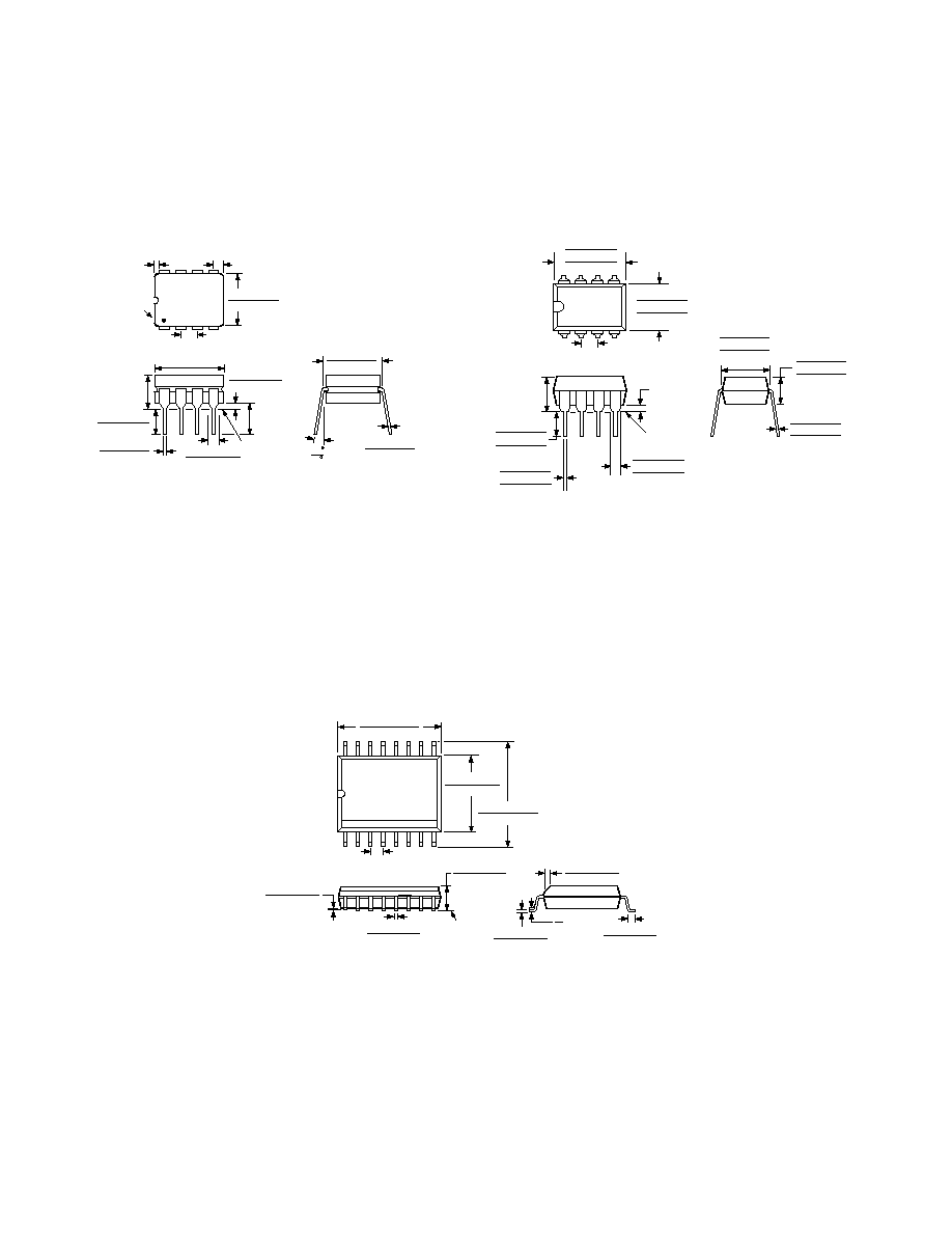
8-Lead Ceramic Dual In-Line Package [CERDIP]
Z-Suffix
(Q-8)
Dimensions shown in inches and (millimeters)
1
4
8
5
0.310 (7.87)
0.220 (5.59)
PIN 1
0.005 (0.13)
MIN
0.055 (1.40)
MAX
0.100 (2.54) BSC
15
0
0.320 (8.13)
0.290 (7.37)
0.015 (0.38)
0.008 (0.20)
SEATING
PLANE
0.200 (5.08)
MAX
0.405 (10.29) MAX
0.150 (3.81)
MIN
0.200 (5.08)
0.125 (3.18)
0.023 (0.58)
0.014 (0.36)
0.070 (1.78)
0.030 (0.76)
0.060 (1.52)
0.015 (0.38)
CONTROLLING DIMENSIONS ARE IN INCHES; MILLIMETERS DIMENSIONS
(IN PARENTHESES) ARE ROUNDED-OFF INCH EQUIVALENTS FOR
REFERENCE ONLY AND ARE NOT APPROPRIATE FOR USE IN DESIGN
OUTLINE DIMENSIONS
8-Lead Plastic Dual In-Line Package [PDIP]
P-Suffix
(N-8)
Dimensions shown in inches and (millimeters)
SEATING
PLANE
0.180
(4.57)
MAX
0.150 (3.81)
0.130 (3.30)
0.110 (2.79)
0.060 (1.52)
0.050 (1.27)
0.045 (1.14)
8
1
4
5
0.295 (7.49)
0.285 (7.24)
0.275 (6.98)
0.100 (2.54)
BSC
0.375 (9.53)
0.365 (9.27)
0.355 (9.02)
0.150 (3.81)
0.135 (3.43)
0.120 (3.05)
0.015 (0.38)
0.010 (0.25)
0.008 (0.20)
0.325 (8.26)
0.310 (7.87)
0.300 (7.62)
0.022 (0.56)
0.018 (0.46)
0.014 (0.36)
CONTROLLING DIMENSIONS ARE IN INCHES; MILLIMETER DIMENSIONS
(IN PARENTHESES) ARE ROUNDED-OFF INCH EQUIVALENTS FOR
REFERENCE ONLY AND ARE NOT APPROPRIATE FOR USE IN DESIGN
COMPLIANT TO JEDEC STANDARDS MO-095AA
0.015
(0.38)
MIN
16-Lead Standard Small Outline Package [SOIC]
Wide Body
S-Suffix
(RW-16)
Dimensions shown in millimeters and (inches)
CONTROLLING DIMENSIONS ARE IN MILLIMETERS; INCH DIMENSIONS
(IN PARENTHESES) ARE ROUNDED-OFF MILLIMETER EQUIVALENTS FOR
REFERENCE ONLY AND ARE NOT APPROPRIATE FOR USE IN DESIGN
COMPLIANT TO JEDEC STANDARDS MS-013AA
SEATING
PLANE
0.30 (0.0118)
0.10 (0.0039)
0.51 (0.0201)
0.33 (0.0130)
2.65 (0.1043)
2.35 (0.0925)
1.27 (0.0500)
BSC
16
9
8
1
10.65 (0.4193)
10.00 (0.3937)
7.60 (0.2992)
7.40 (0.2913)
10.50 (0.4134)
10.10 (0.3976)
0.32 (0.0126)
0.23 (0.0091)
8
0
0.75 (0.0295)
0.25 (0.0098)
45
1.27 (0.0500)
0.40 (0.0157)
COPLANARITY
0.10

REV. C
OP270
≠15≠
Revision History
Location
Page
4/03--Data Sheet changed from REV. B to REV. C.
Deletion of OP270A model . . . . . . . . . . . . . . . . . . . . . . . . . . . . . . . . . . . . . . . . . . . . . . . . . . . . . . . . . . . . . . . . . . . . . . . . . .Universal
Edits to FEATURES . . . . . . . . . . . . . . . . . . . . . . . . . . . . . . . . . . . . . . . . . . . . . . . . . . . . . . . . . . . . . . . . . . . . . . . . . . . . . . . . . . . . . 1
Edits to CONNECTION DIAGRAMS . . . . . . . . . . . . . . . . . . . . . . . . . . . . . . . . . . . . . . . . . . . . . . . . . . . . . . . . . . . . . . . . . . . . . . . 1
Changes to SPECIFICATIONS . . . . . . . . . . . . . . . . . . . . . . . . . . . . . . . . . . . . . . . . . . . . . . . . . . . . . . . . . . . . . . . . . . . . . . . . . . . . 2
Deletion of WAFER LIMITS and DICE CHARACTERISTICS . . . . . . . . . . . . . . . . . . . . . . . . . . . . . . . . . . . . . . . . . . . . . . . . . . . 4
Changes to ABSOLUTE MAXIMUM RATINGS . . . . . . . . . . . . . . . . . . . . . . . . . . . . . . . . . . . . . . . . . . . . . . . . . . . . . . . . . . . . . . 4
Changes to ORDERING GUIDE . . . . . . . . . . . . . . . . . . . . . . . . . . . . . . . . . . . . . . . . . . . . . . . . . . . . . . . . . . . . . . . . . . . . . . . . . . . 4
Changes to equations in Noise Measurements section . . . . . . . . . . . . . . . . . . . . . . . . . . . . . . . . . . . . . . . . . . . . . . . . . . . . . . . . . . . 10
Change to Figure 10 . . . . . . . . . . . . . . . . . . . . . . . . . . . . . . . . . . . . . . . . . . . . . . . . . . . . . . . . . . . . . . . . . . . . . . . . . . . . . . . . . . . . 11
Updated OUTLINE DIMENSIONS . . . . . . . . . . . . . . . . . . . . . . . . . . . . . . . . . . . . . . . . . . . . . . . . . . . . . . . . . . . . . . . . . . . . . . . 14
11/02--Data Sheet changed from REV. A to REV. B.
Updated ORDERING GUIDE . . . . . . . . . . . . . . . . . . . . . . . . . . . . . . . . . . . . . . . . . . . . . . . . . . . . . . . . . . . . . . . . . . . . . . . . . . . . 15
9/02--Data Sheet changed from REV. 0 to REV. A.
Edits to ABSOLUTE MAXIMUM RATINGS . . . . . . . . . . . . . . . . . . . . . . . . . . . . . . . . . . . . . . . . . . . . . . . . . . . . . . . . . . . . . . . . . 5
Edits to ORDERING GUIDE . . . . . . . . . . . . . . . . . . . . . . . . . . . . . . . . . . . . . . . . . . . . . . . . . . . . . . . . . . . . . . . . . . . . . . . . . . . . . 15

≠16≠
C00325≠0≠4/03(C)
Document Outline